Assembly instructions for the MOTM version of the Blacet Time Machine
If you have decided to build the Blacet Time Machine and convert it to the MOTM format, you have no
doubt found that this procedure is more complicated than simply purchasing and building a Synthesis
Technology MOTM kit. And, you have found that Blacet’s concept of "MOTM versions" of his kits is
simply omission of the parts you would not use. The additional parts you need are not included. The
instructions are not revised to reflect the changes involved in conversion to the MOTM format. Instead
of having everything you need delivered to your door in one neat package, you must accumulate parts
from a variety of sources. Here is what you need to get started:
I will not attempt to list the part numbers here. Changes and a variety of vendors and suppliers make that
task unreasonable to include in the assembly instructions. Instead, I will refer you to "the" definitive MOTM
compatible parts reference assembled by Dave Bradley. Visit http://www.hotrodmotm.com/parts_list.htm
for everything you need to know about where to get these parts.
You will also need to refer to your original Blacet assembly instructions for the graphics including the
schematic and PCB drawings. I cannot include those in this document without infringing on John’s
copyright (which, of course, I would not do).
Please be aware, that these instructions include some modifications to the original Time Machine. I have
included all of the changes recommended by John since the new Time Machine was issued. In addition, I
have included the documentation for each of three modifications. You can decide if you want to make the
modifications and following the instructions accordingly. The first modification is to add a manual bypass
switch to the front panel. This has the same effect as canceling with the cancel CV input (which we have
renamed "bypass" on the Stooge panels). If you choose not to implement this bypass switch, simply leave
the switch and resistor off.
The second modification is designed to protect two of the inputs from negative voltage input which has
proven to lock up the clock. These changes involve the Delay CV and External Mod CV inputs.
Before we begin with the electrical construction, you have some mechanical issues to deal with. My PCB
mounting brackets are universal and are not specifically made for a certain PCB. Some modifications are
required to the four-pot long mounting bracket to work for this assembly. I have taken several photos of the
construction process for my Time Machine. You will find relative hypertext links to the photos throughout
these instructions in the HTML version. If you are reading the HTML version of this document on-line at
www.wiseguysynth.com, these links will take you directly to the photos. If you have saved the HTML
document to your hard drive for reference, you will need to save each photo to the same directory as this
document. The photo links will then work for you off-line. You can take a quick tour of all photos here. MS
Word and text users need to view photos separately (as indicated by "photo ##" throughout the text).
The only modification needed to the four-pot long bracket is drilling the PCB mounting holes. Unfortunately,
the Blacet Time Machine PCB does not include any mounting holes. So, you must drill your own holes in
the PCB also. And, the PCB is very densely populated. So, great care must be exercised in selecting the
location of your holes. You need to be absolutely certain that no traces are cut and that the screw heads
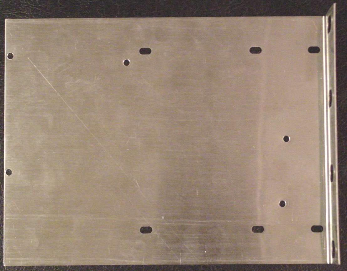
will not interfere with the part on top. After careful consideration, I drilled 5 holes in my Time Machine panel
for support. You can see my choices for holes in my photo (01).
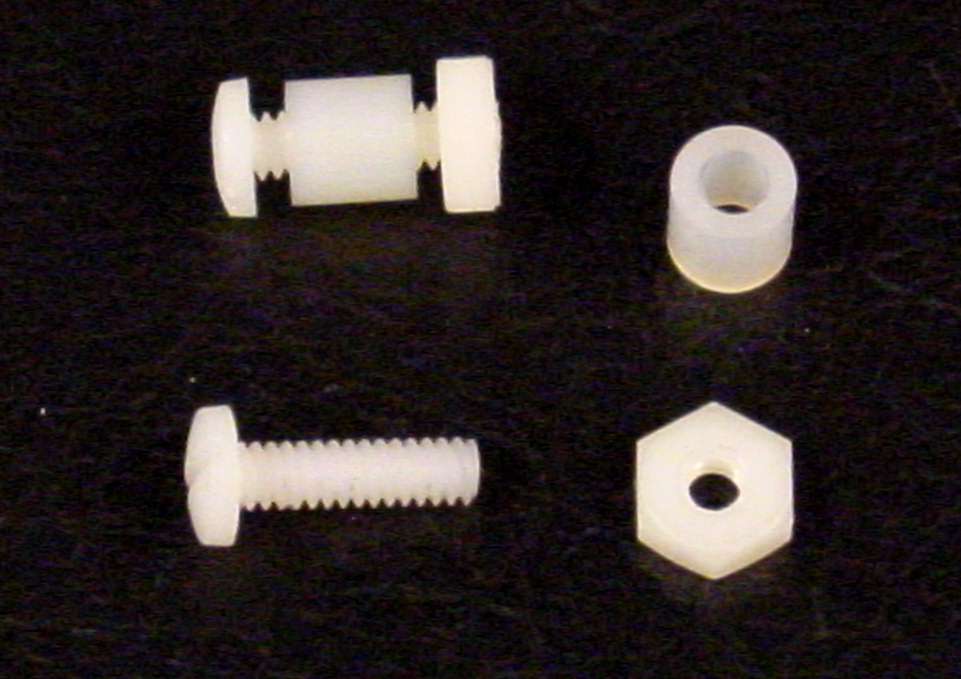
Nylon machine screws, standoffs and nuts are essential as there are no locations to drill that will provide
enough physical clearance for metal ones. These can be found in the specialty hardware section of most
home improvement type stores. I expect they can be found in many hobby stores also. I used #6-32 nylon
hardware. However, I probably would have used #4-40 if I could have found it when I was picking up my
parts. The correct hole size for #6-32 is 9/64 inch. I highly recommend you start with a very small bit to
place the hole and then drill the smaller hole out to the 9/64 finished size. Photo (02)
You must drill the PCB first. After you have it drilled, then you can decide how you want it positioned on
the bracket. If I had known anything about the size of the PCBs that would someday find their was onto
my long brackets, I would have made them about ½ inch deeper. The holes at the rear of the PCB are
right at the edge. See
You must drill the holes in the bracket that are aligned with your PCB holes. I offer the following
suggestion. Place masking tap on your bracket in the general locations where you can see the holes
will be needed. Position your PCB on top of the bracket exactly as you wish it to be mounted (without
the stand offs of course). Don’t forget to leave room for your pots. You can take a fine point pen and
trace circles inside the newly drilled PCB holes onto the masking tape. Now, you have your holes
marked on your bracket exactly where they need to be. Drill your holes with the size but appropriate
for your hardware. 9/64 is perfect for # 6-32.
I have my PCB on the left side (looking from the back) like MOTM modules. However, it will work either
way. Putting it on the left as I did causes the PCB to be upside down from its original configuration.
However, since no pots are board mounted, it really makes little difference. I think upside down is
best actually.
This might be a good spot to make sure all your mechanical parts go together well before you move to
soldering. Mount your PCB to your bracket using stand offs. Attach your bracket to your front panel using
two of the four pots. Do not forget to install backing nuts on your pots. This is CRITICAL. The concept of my
mounting brackets is that the bracket is held in place by sandwiching the bracket and front panel together
between the back nut and front nut on the pot shaft. You cannot tighten against the pot body. You will have
nothing but trouble if you try. You should always use backing nuts on your pots. Hopefully, everything fits
together well in your trial fitting and you are ready to heat up the soldering iron.
I will also note here, that my brackets were made and sized before I knew there was going to even be a
Time Machine. So, they are just barely long enough. In fact, to be sure I had plenty of room, I specially
selected 148 or 149 series pots for the locations in front of the PCB. For the two not in front of the PCB,
you can use any size 50 K pot. In my photos you will find the larger Bournes pots in these locations (cause
I have about 10 of them in my personal stock). You will also notice my REGEN pot is a carbon pot. I really
did not want to use any carbon pots. But, this is the only one I found with a center detent. Dave Hylander
actually found it and shared his information with me. You can see the difference in fitting room in these
photo comparisons:
I am not including part numbers for pots. Use what suits your needs. If you want to know what part numbers
I used, just drop me and note and I will give you the exact part numbers.
I will confess that I have been spoiled by the completeness of MOTM assembly instructions. The Blacet
instructions are not nearly as complete, leaving the assembler to jump back and forth between the
schematic and parts list to figure out what part goes where. As I write these instructions for the conversion
to the MOTM format, I am also adding to the Blacet document some more specific instructions that I
believe are easier to follow. I also changed the relative order of the component placement on the PCB.
First, a word about solder. I am assuming that you will follow the MOTM solder standard and use organic
solder (requiring a board wash) for much of the soldering, and then switching to a no-clean solder to
complete the construction. If you adopt another strategy, you are on your own concerning the need to
wash the PCB.
I like to install my components based on relative height. It seems to be easier for me. However, feel free to
jump around the instructions to suit yourself. I started with the individual resistors. However, I skipped over
the resistors that stand on end until later.
PART 1: Installing the individual resistors (only those that lay flat) and diodes
You will use organic washable solder for this part of the construction.
First, the 1% tolerance blue resistors:
NOTE: OK, here is a spot for the modification that protects the clock from lock-up from negative
control voltage. This one protects both the Delay CV and External Mod CV input. If you want to skip
my modification, install R11. If you want to add my modification, just leave R11 out at this time. Put
it aside for later installation.
Now, the 5% tolerance resistors:
That completes the installation of all the individual resistors positioned flat on the PCB. Next, you will add
the diodes. Please note that two different diode types are used in the Time Machine. Use care not to
confuse them. And, be certain to note polarity. The arrow on the PCB points toward the stripe on the diode.
PART 1 continued: Installing the non-electrolytic capacitors
This completes the installation of all capacitors except the larger electrolytic. Do not confuse the PS1
and PS2 resettable fuse-like devices as capacitors. They resemble small ceramic capacitors but are
distinguished by preformed leads and are marked "R010BOVS." You will install those later.
OK. This is a good stopping point for your first board wash. Run the board under warm water (do not use
any soap or cleaners). Gently scrub both sides of the board to remove the organic flux. Any small brush will
do the job. I use an old toothbrush.
If you have not done so already, this would be a good time to inspect your solder joints. Check to be certain
you have not forgotten to solder one end of a component or that you have not accidentally bridged one
thing to another with excess solder. Personally, I check my joints right before I clip my leads. It seems
easier to me to find what I have just competed that way. Here is what your PCB should look like:
PART 2: Installing resistor networks, sockets, transistors and regulators.
Next you will install the resistor networks. Notice that each resistor network has a white dot on one end.
Be absolutely certain to align the resistor networks on the PCB so the white dot is at the end indicated
by the white dot on the PCB. Before you insert your resistors, check that the pins are not bent. Bend them
as needed to form a straight line.
Cinch resistor networks to the PCB by bending the end pins over, one in one direction and the opposite
end the other direction. Then, solder a couple of pins and inspect to be sure you are happy with the
position. Straighten the bent-over pins and solder all remaining pins.
Next, you will install the sockets. Notice that 8 pin, 14 pin, and 16 pin sockets of the same width are used.
Be certain not to place a shorter socket in the wrong location in place of a longer one. I like to start with the
longer ones. Then, I know I cannot make that mistake. The PCB indicates the end for the notch. Align the
socket notch as marked on the PCB. Bending two opposite corner pins is a good way to hold the socket
to the PCB wile soldering. Solder the other two corner pins ONLY. But, before soldering, make sure all the
pins are coming through the holes in the PCB. These pins bend easily and could bend back under the
socket and go unnoticed. Check the socket flat on the PCB while it is still easy to re-heat one pin and
squeeze the socket to the PCB if it is not perfectly flat. Once you are certain the socket is flat, solder the
remaining pins.
Notice that the socket for U3 has only 8 holes on the PCB for pins. You will use one of the 14 pin sockets
but clip out the 3 middle pins on each side, leaving 4 pins per side (2 at each end). Then, the socket will
fit the PCB.
Next, you will install the transistors and voltage regulators. Notice the orientation (flat side) of each (except
Q1) is marked on the PCB. Be sure to face them in the correct direction. These devices will not be pushed
all the way down on the PCB. Leave ¼ inch or less between the bottom of the transistor and the PCB.
Cinch the device by bending the outside leads, then solder the middle terminal only. Then, straighten the
leads and the transistor and solder the remaining two leads. Transistor Q1 is actually a transistor pair. Its
tab orientation is marked on the PCB.
OK. This is a good stopping point for another board wash. Run the board under warm water (do not
use any soap or cleaners). Gently scrub both sides of the board to remove the organic flux. This is
board wash 2 of 3.
If you have not done so already, this would be a good point to inspect your solder joints. Check to
be certain you have not forgotten to solder one end of a component or that you have not accidentally
bridged one thing to another with excess solder. Verify the polarity of diodes. Check that the transistors
and regulators are installed with the flat side as marked on the PCB. Your PCB should look now look something like this (photo 07).
PART 3: Installing the remaining components on the PCB
In this part you will complete the installation of components on the PCB. Along the line you will encounter
your last board wash and switch to a no-clean solder. For now, we are still using organic solder that
requires a board wash.
Due to space limitation on the PCB, many of the resistors stand on one end instead of laying flat on the
PCB. They take less PCB space, but stick up much higher and are easier to inadvertently bend. I have
saved these stand up resistors until now when we installing the taller PCB components. Notice that one
of the terminal has a circle around it. The end of the resistor will sit in this circle with the bent lead in the
other hole.
You will start with the remaining 1% resistors
Next, the remaining 5% resistors:
note - In the photos of my PCB, you will notice that R32, R33, R34, R35, and R44 5% resistors are
actually changed to1%. That is just my personal preference to metal film resistors in regulator circuits.
Important: When you trim your leads after soldering do NOT trim the lead off of R42 (the end that sits in
the circle on the PCB). Instead, just bend that lead over. Later, we will use this as an attachment point for
the bypass switch modification. Here is a photo (08) of both untrimmed leads (this one and another later).
For the last resistor R36, the size of the resistor varies depending on the type of LED you plan to use.
If you are using the LED supplied with the Blacet kit, use 5.6K ohm. If you are using the MOTM style
Lumex LED, use a 3.3K ohm resistor. Note: Resistor position R11 still remains open if you are installing
my negative CV voltage protection)
Now all resistors except the temperature compensating resistor R7 have been installed. R7 will be the
last component.
Next, you will install the remaining capacitors. All remaining capacitors are electrolytic and polarity must
be observed. Notice the PCB is marked with a "+" sign. The caps have "+" indicated by a longer lead
and "-" indicated by a stripe on the capacitor. Install all capacitors with the "-" stripe facing away from
the "+" mark on the PCB.
These are the last three components to be attached to the PCB with organic washable solder. After
these, you will be ready for your final board wash and a break.
Important: When you trim your leads after soldering do NOT trim the lead off of PS1 (the end toward
capacitor C31). Instead, just bend that lead over. Later, we will use this as an attachment point for the
bypass switch modification. Here is a photo (08) that show both untrimmed leads.
NOTE: Be sure when you are fitting your power connector that you have room to fit your screw if you
placed one in this corner as I did. While all fit the connector the same, I have found that Blacet has used
a variety of 156 style power connectors. Some have a larger base than others. Make sure your base
does not prevent the installation of your nylon support screw. If it does, use the MOTM style part number
as indicated on Moe’s MOTM compatible part number page. Those fit just fine. Some of the Blacet
power connectors are OK, some are not.
OK. It’s time for the last board wash. Run the board under warm water (do not use any soap or cleaners).
Gently scrub both sides of the board to remove the organic flux. On-end resistors are more easily bent
so, be extra careful on the top board scrubbing. You will NOT use washable solder for the remainder of
construction.
If you have not done so already, this would be a good point to inspect your solder joints. Check to be
certain you have not forgotten to solder one end of a component or that you have not accidentally bridged
one thing to another with excess solder. Verify the polarity of all electrolytic capacitors. Yes, you still have
those two untrimmed leads. J
Allow your PCB to dry completely, and put away that organic solder. All soldering from this point forward
will make use of no-clean solder.
PART 4: Installing the trimmer pots, R7, and connecting wires to the PCB
The six trimmer pots and temperature compensating resistor are the last components to be soldered to the
PCB. Notice that the trimmers have varied values. Be certain to get the correct value in the correct location.
Check their value with your meter if you have any doubt. Don’t forget to switch to no-clean solder.
Now, I will refer you back to Part # 1 of these instructions. If you did choose to make my negative control
voltage protection modification, you have left out part R11 (45.3 K ohm resistor. Here is where we will
install the modification, that does include that resistor. Insert part only one end of R11 (45.3K ohm) so
that it is in a standing position.
Insert R11 in the hole that is closest to Q1. At the opposite hole (toward the edge of the PCB), insert your
extra 1K ohm 1% resistor also standing on end. Now, tie together by twisting the two tops of these two
resistors. They now have a tee pee style appearance on the PCB. Do not solder the tops together yet.
Do solder to PCB.
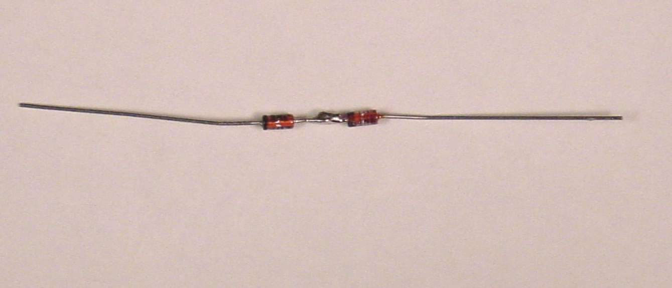
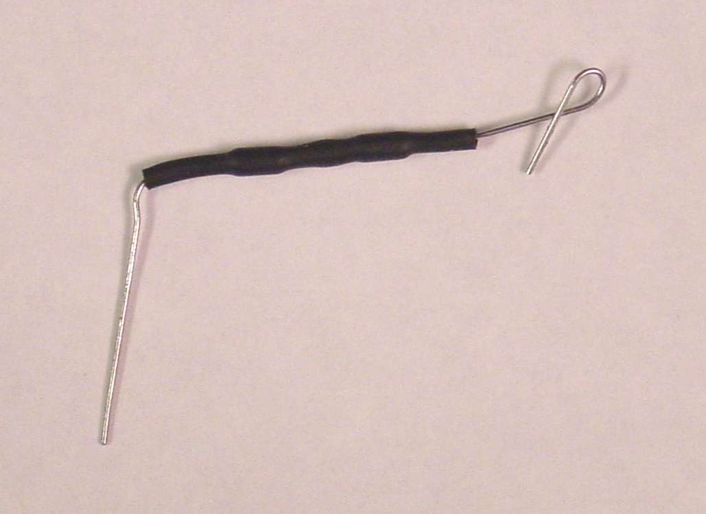
Take your two remaining 1N4148 signal diodes and connect them end to end about ½ inch apart
(removing a significant portion of their leads), Connect so that one cathode connects to one anode,
or so the cathode stripes are both facing the same direction. photo (13) I stuck about 1 ½ inches of
heat shrink over this so that I end up with a component inside (composed of two diodes in series) and
I have a nice long lead sticking out of each end. The heat shrink is not required, but makes the modification
bullet proof in my opinion. If you do add the heat shrink, be sure to mark which end is the cathode.
photo (14)
Now, you are ready to install your diode combo. The anode end connects to the twisted junction point of
R11 and the 1K resistor that stands on end tee pee style at the R11 location. The cathode lead connects
through the via hole just below R14 and just above the "S" in RESEARCH. This location is electrically
ground. Now you can solder the top connection of R11, the 1K resistor and the anode end of your series
diodes. Your finished modification should look like this
Now, you have come to the last part on the PCB – the temperature compensated resistor R7. This resistor
is installed so that it sits on top of Q1. It must make good thermal contact with Q1. You need to use some
thermal joint compound. Put a dab on top of Q1. Be careful not to use too much. This stuff is messy and you
want it contained to only the top of Q1.
Form your leads and insert 1K resistor R7 so that the resistor body is flat on top of Q1 resting on the
thermal compound. Bend the resistor leads under the PCB to hold into place. Solder one side only. Then,
gently pull any slack out of the other lead with needle nose pliers to pull the resistor firmly on top of Q1.
Re-bend the lead to hold into position and solder. Your Q1 / R7 combo should now look like
Congratulations. You are complete with all soldering of components to the PCB. Up until this point, you
have basically built the PCB as if it were going behind the Blacet panel (except you did not attach the
six front panel pots or LED to the PCB). From this point forward, you will be departing considerably from
the Blacet version of the Time Machine to attach to the MOTM style front panel. I will assume at this point
that you already have your MOTM style front panel drilled and ready to go. I will also assume you have your
bracket drilled for the PCB. Your completed PCB should resemble
Your next task, is to prepare the front panel controls for attachment to the PCB. You will also attach all wires
to the PCB as needed. Gather up your six 50 K linear pots, nine ¼ jacks, one SPDT switch, and LED.
I decided to prepare my front panel controls by attaching all the wires of the correct length to facilitate the
attachment to the PCBs. I also decided to adopt a color standard for the pot and switch numbers. I highly
recommend this. I will often refer to the colors I used. Be sure to write down the color selections you decide
to use.
For my standard for pots and switches, I elected to use these colors (I used some of he wire John supplied
with the kit): Pin 1 = green/white/black striped, Pin 2 = blue, Pin 3 = yellow/white striped. Please be aware
that all of the wire lengths I specify in this document assume a PCB mounted to the left (looking from the
back). Opposite side mounting will change these recommended lengths.
First, attach three wires to each 50 K panel pot. Be sure you have a backing nut for all six of the pots. If you
use pots intended for PCB mounting (as I did), use heat shrink to insulate the wires connected to the pots.
Twist your pot wires together to keep everything neat. Your pots should look like this:
photo (18)You will not attach wires to the switch and LED. Instead, these wires will first be connected to the PCB
along with the jack wires. Then, the wires will be attached to the switch and LED after you have mounted
the all components to the front panel.
There is no need to prepare any jacks for the front panel. We will actually start those wires from the PCB
end. Let’s do that now. Before we do though, you must do some advance planning for color and wire
length. I will report to you the colors and lengths I used. I highly recommend you make yourself a list and
a drawing of the back of the panel showing which jack is in which location. Starting from the top, left to
right from back: Bypass = J2, Depth = J6, Rate = J4, Mod Rst = J5, Ext Mod = J7, Out = J9, Regen = J3,
delay = J1, and In = J8.
You also must decide if you will route these wires from the top of the PCB or from the bottom. The bottom
is much more difficult but produces a very neat appearance when done. If you do route them across the
bottom, plan to put them in heat shrink or otherwise protect them from the sharp points of cut off leads on
the bottom of the PCB. The wire lengths should not significantly change from top to bottom. You may find
my recommended lengths a little long depending on how you route your wires. However, I measured for
the worst case. Better too long than too short. Now, we are ready to attach PCB wires for jacks, LED,
and switch.
Let’s do the switch leads first. Remember those two leads you did not clip off way back when we were
attaching components to the PCB. You should have a lead hanging out from one end of R42 and one
end of PS1. These are the connection points for your switch leads. These wires should be about 11" long.
Polarity and color are not important. I used blue and yellow. Attach the wires to the component leads about
3/8 inch to ½ inch away from the PCB This way, the solder from this connection will not run into the PCB
solder joint. It is more flexible if you do this. Install heat shrink over both of these joints right down to the
PCB so there is no chance of the leads shorting to anything else on the PCB. We will wire these to the
switch later. Here is a
Next, you will attach the two 5 inch leads to the PCB for the LED. These are located on the PCB between
pot locations R2 and R3. You can attach wires up or down. Either works fine. Down requires the longer
length I specify. Be sure to color code these and write it down. I attached red to the anode and black to
the cathode connection.
Attach 6 wires (I used black) to the "COM" connection by the power connector. These leads must be at
least 13 inches long. You will also attach ten more wires to the jack connectors on the PCB (J1 through
J9, and J7S).
I used different colors for each as much as possible to make it easy to follow. Use whatever colors you
want. But, be sure to write it down. You will likely tie many of these wires together and knowing which
color goes to which will be very beneficial.
Cut the following wire lengths and attach to the PCB:
J1 – 5 inches – I used blue (separate bundle – see photo)
J2 – 11 inches - I used green
J3 – 8 inches - I used yellow
J4 – 12 inches - I used red
J5 – 13 inches - I used white
J6 – 10 inches - I used blue
J7 – 12 inches - I used green / black / white stripe (Blacet wire)
J7S – 12 inches - I used yellow / white stripe (Blacet wire)
J8 – 12 inches - I used green (separate bundle – see photo)
J9 – 12 inches - I used yellow (separate bundle – see photo)
I brought mine all out the bottom and used heat shrink to organize them. See
photo (17).Part 4: Attaching front panel controls and wiring to the PCB
Instead of trying to connect wires to the front panel after parts are attached to the panel (as common on
some MOTM construction), you will wire your pots to the PCB first and then attach to the front panel when
mounting the PCB. I think this is easiest for this module. And, that is why you prepared the pots with leads.
Connect the pots to the PCB. Be certain that the terminal numbers on the pots match those on the PCB.
Notice that terminal 1 is marked at each pot location. Following my color standard, pin 1 = green / white /
black striped, pin 2 = blue, pin 3 = yellow/white striped. Yours may vary. Since this is a double sided PCB,
the pot leads can be soldered so that the wires come from the top (soldered normally from bottom) or
come from the bottom (soldered from the top side). Either works. I will report the way I did mine in an
effort to reduce wire clutter. You may vary according to your own desires.
My pots R2 and R4 were connected so that the leads exit the bottom of the PCB and solder from the top.
The remaining four were soldered so the wires exit form the top and were soldered normally from the
bottom. If you have not done so already, twist the pots around so that all the leads between the PCB
and the each pot are neatly twisted together. Here is what mine looked like
Part 5: Attaching to front panel
You have many wires on your Time Machine panel now. I find it helpful to pull back and tie out of the way
the ones not being used. Front panel attachments will start with the pots. Four of the pots will hold the PCB
mounting bracket to the front panel. I am assuming you are following my lead to have the PCB on the left
side as you look from the back (MOTM style). Adjust accordingly if you have selected the opposite side.
Be absolutely certain to use the backing nuts on your pots. You cannot tighten against the pot. This will
ruin the pot.
Your circuit now attached to the panels should look like this:
photo (20)Pull the two wires for your LED through the LED hole in the front panel. Slide some heat shrink as needed
over the two wires before you attach them to the LED. Solder the wires so that the anode wire goes to the
longer of the two leads on the LED. According to my color selection, my red wire connects to the longer
lead and my black wire to the shorter lead. Heat to shrink and push the LED into the panel hole.
Now that you have the LED installed, insert and tighten the last remaining jack in the bypass jack location.
We left this out to make it easier to install the LED.
Next, you will attach the wires to the jacks. First, you will notice that while you have 9 jacks, you have only
6 "common" black wires for grounds. Some of the jacks share a common ground wire. The following jacks
(J1 delay, J3 regen, J4 rate, J6 depth) have their grounds connected together and attached to the PCB
with a single common wire. All ground wires attach to the bevel side of the jack. The remaining 5 common
wires attach to the remaining 5 jacks (J2 bypass, J5 mod rst, J7 ext mod, J8 in and J9 out).
You have 10 wires remaining to connect to the 9 jacks.
Your last connection to the front panel is to the bypass switch modification. Of course, if you have not
elected to include the bypass switch modification, you are done. But, I expect most of you are including this
modification since the screening is included on the Stooge Panel. You will need to your switch and a 100K
resistor. I mounted my switch to the panel after I connected the wires.
Connect one end of the 100K ohm resistor to the back of your switch to one of the end terminals. It does
not matter which end terminal. Slide some heat shrink as needed over the two wires before you attach
them to the switch. Connect these two wires from your circuit board (we wired the PCB end earlier) to your
switch. These should be the last two unconnected wires you have coming from your PCB. One will connect
to the middle lug on your switch. One will connect to the end of the resistor. One end terminal of the switch
remains open. It does not matter which of the two wires connect to the middle terminal. There is no polarity
to this connection.
Insert your switch into the front panel. Position it so that the unconnected lug is toward the top. Be sure to
use the backing nut on the switch. And, do not overtighten. These switches will not tolerate the kind of
torque used to tighten jacks or pots to your panel.
Congratulations. Your Time Machine is now completed except for the chip installation. Add your six knobs
to the panel pots. Your Time Machine is now ready for testing and calibration. Please refer to the Blacet
documentation for testing and calibration. Notice that the first test of the power supply is done without any
chips installed in the sockets. Here are photos of mine:
Once you have verified proper power supply voltages per the Blacet instructions, you can insert the chips
in the sockets. Be certain to exercise static control to avoid damage to the chips. Be sure to install all chips
with the notch toward the front panel.
Follow Blacet’s instructions for calibration and check out. If you do not have a frequency counter to set the
VCO frequency range, you will have to estimate. Set both R1 and R2 near the center of their range. R1 sets
the minimum delay time, R2 sets they maximum. I plan to offer a document for calibrating these trimmers
without a frequency meter. I do have a couple of notes of interest for your calibration:
That concludes my instructions for assembly of the Blacet Time Machine in the MOTM format using Stooge
panels and brackets. I hope my work has made the process more enjoyable for you and helped you to
achieve success. I always welcome feedback and constructive criticism. If you have any ideas for
improvement of this document, please drop me a note. Here are the completed photos.
Larry Hendry
01/26/02
Revision 1