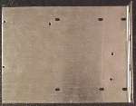
4 pot wide, long version bracket – drill new holes
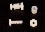
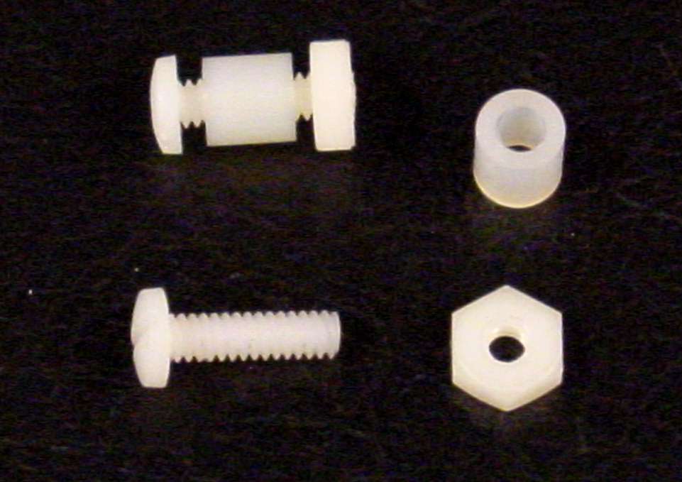
Nylon mounting hardware
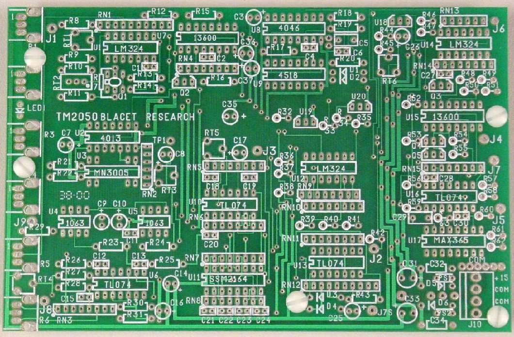
Holes drilled in the PCB for the nylon hardware

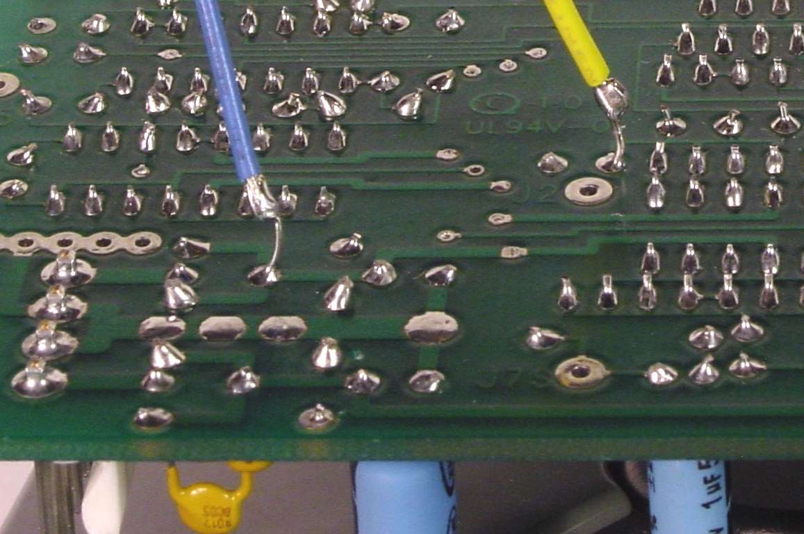
Notice two leads were not trimmed, but rather bent over to avoid trimming. This will be connection for bypass switch mod
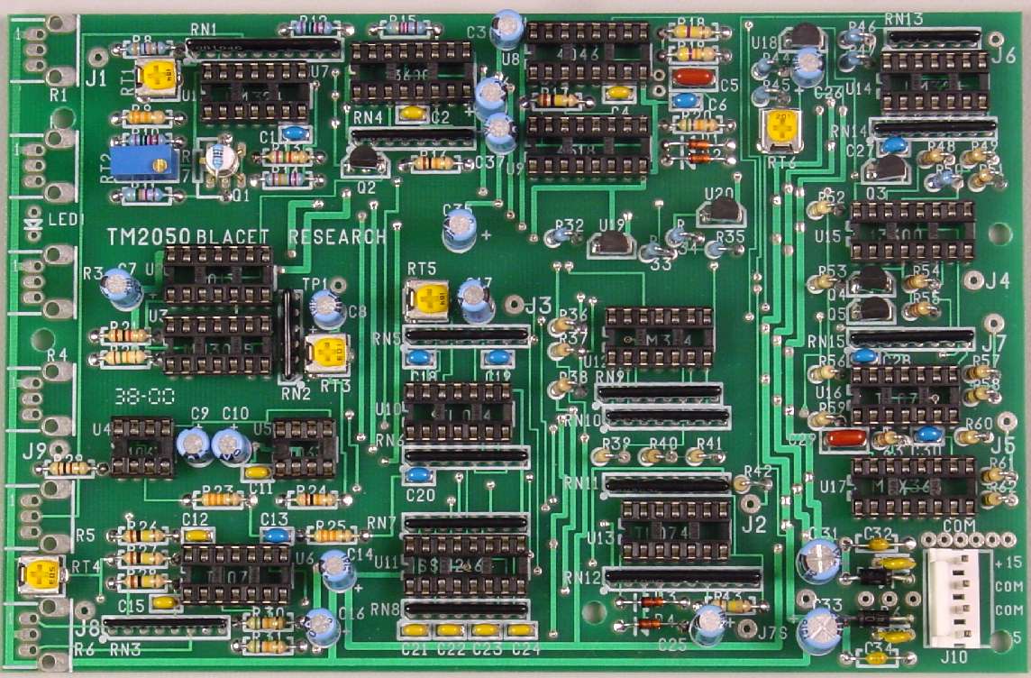
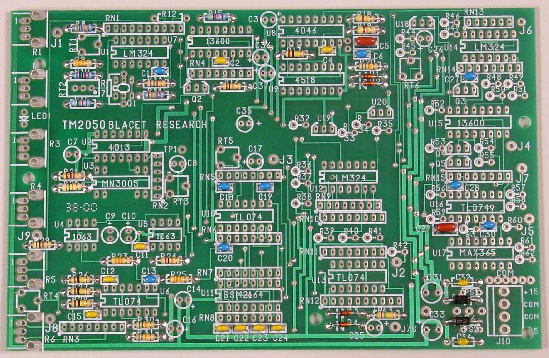
PCB with all components
installed, ready to start attaching wiring. No modifications shown on this one.
Wire attachment for the bypass switch modification. These are connected to those leads we did not trim. Heat shrink required for insulation.
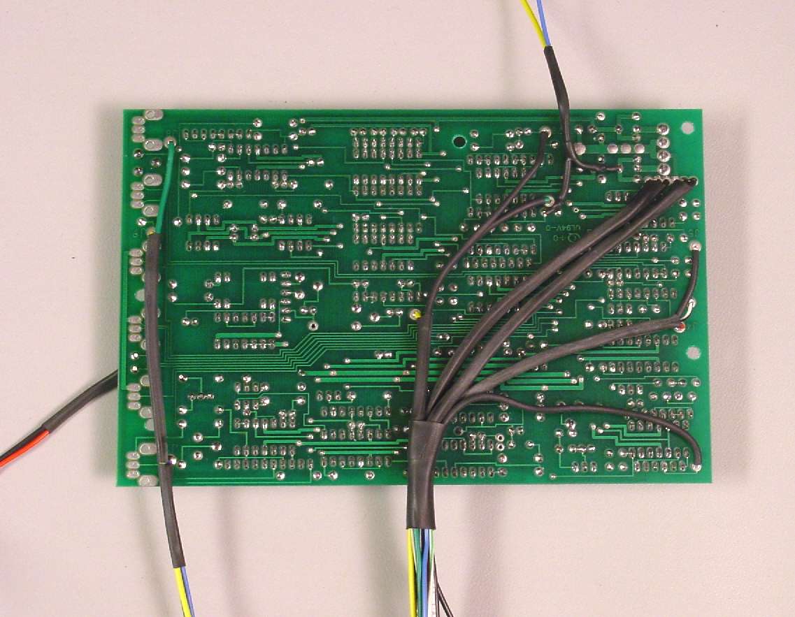
Bottom of PCB after all jack wiring added. LED & bypass switch wiring also seen. Heat shrink added to protect wires from sharp component leads

Bypass jack removed to give access to wiring LED
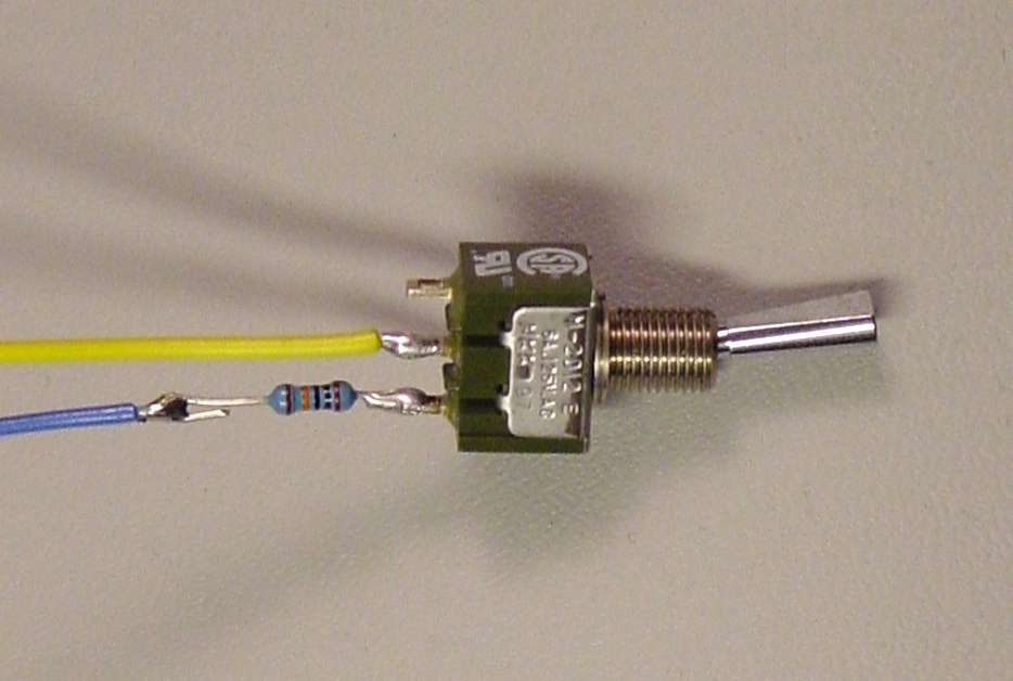
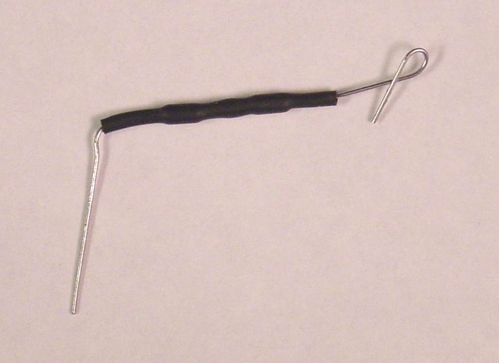
Bypass switch with 100K resistor installed. Need heat shrink to insulate it
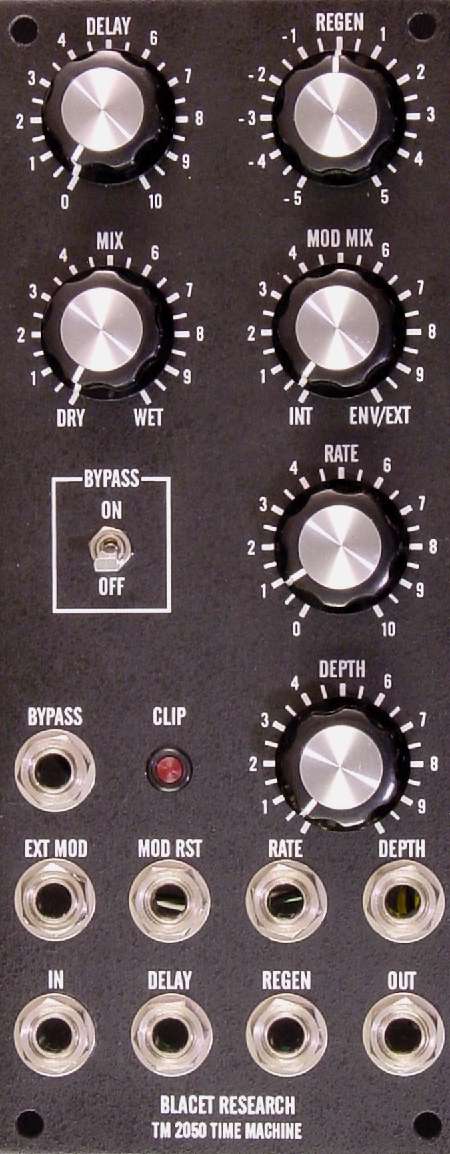
Completed front panel
shown below:

Trial fit with large Bournes pots – not much room between PCB and pots
Trial fit with smaller Spectrol 148 or 149 series pots, and one center detent carbon pot

Detail of tempco resistor
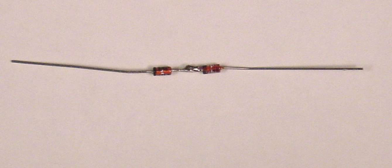
back-to-back diodes for DELAY CV modification
Same diodes with some heat shrink, now ready to install on the PCB
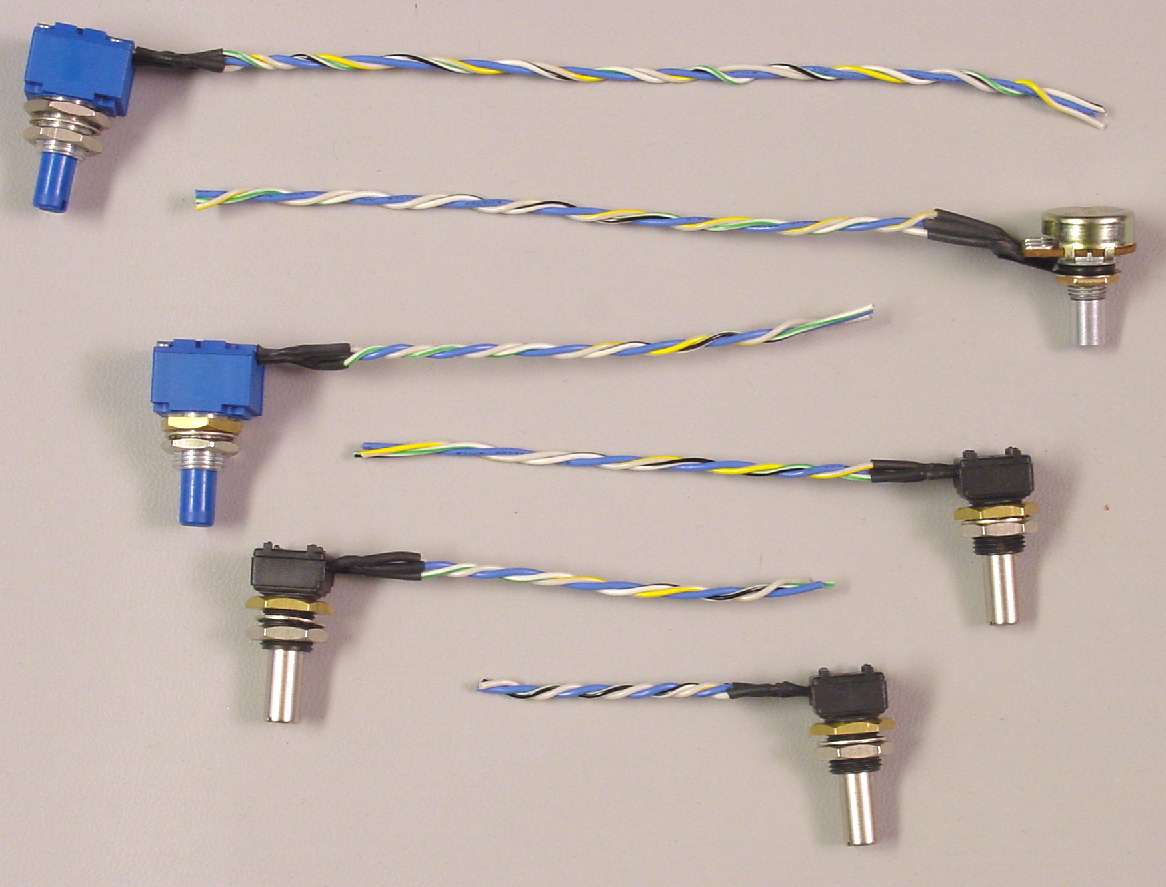
Pots prepared with wire lengths necessary for connecting to PCB

Top of PCB after pots are connected
PCB at first board wash

PCB at second board wash
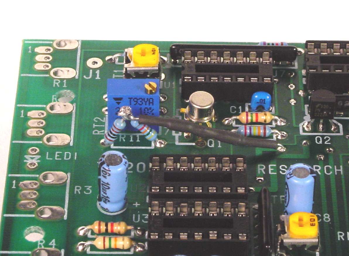
View of the DELAY CV modification 2 diodes & 1K ohm resistor added
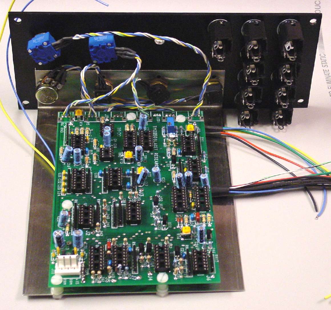
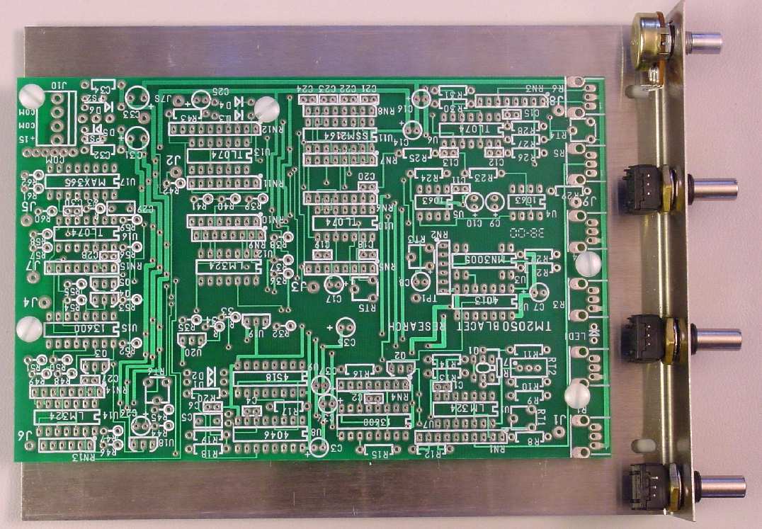
Bracket and PCB mounted to front panel using 4 pots
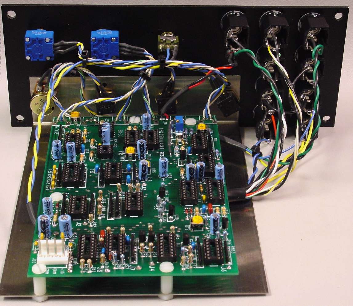
Completed module shown from the back. Chips are not yet installed. Blacet recommends some voltage checks and adjustment on first power up before installing chips.